RESEARCH
Note: A webpage is often more a reflection of past and of some current projects. For details on our future research directions, please contact Peter Kinget.
RESEARCH PROJECTS
CURRENT
|
PASTHigh Performance Phase-locked Loops
High Performance Integrated Oscillators Area Reduction of RF circuits Device Mismatch Ultra-wideband Circuits for Pulse Radio Energy Harvesting Active Networked Tags Ultra-Low Power Pulse Radios Design of Highly Efficient Power Conversion Systems using Meta-Capacitors Digital-Assisted RF Ultra-Low Power Wake-Up Radios Injection-Locking of Oscillators and its Applications Flexible Radio Architectures for Cognitive Radio |
RESEARCH RESOURCES & FACILITIES
CHIP FABRICATIONWe have access to a number of different semiconductor processes for the fabrication of our circuits through a fabrication service provides (e.g., MOSIS, Europractice) as well as through direct relationships with companies and foundries. We currently mainly use 90nm CMOS, 0.13um CMOS, 0.18um CMOS and 0.25um/40GHz BiCMOS processes and are initiating our work in 65nm and 45nm CMOS processes. Take a look at our Chip Gallery!
|
COMPUTING & CAD TOOLSWe use a full set of industrial grade design tools for our IC designs. This includes tools suites from Cadence, Mentor and Agilent. We use PC desktops running Linux as well as servers running CentOS and Linux.
|
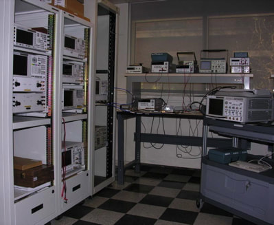
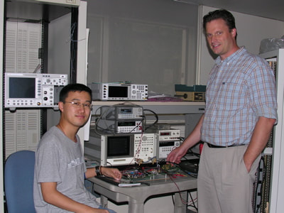
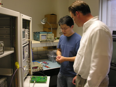
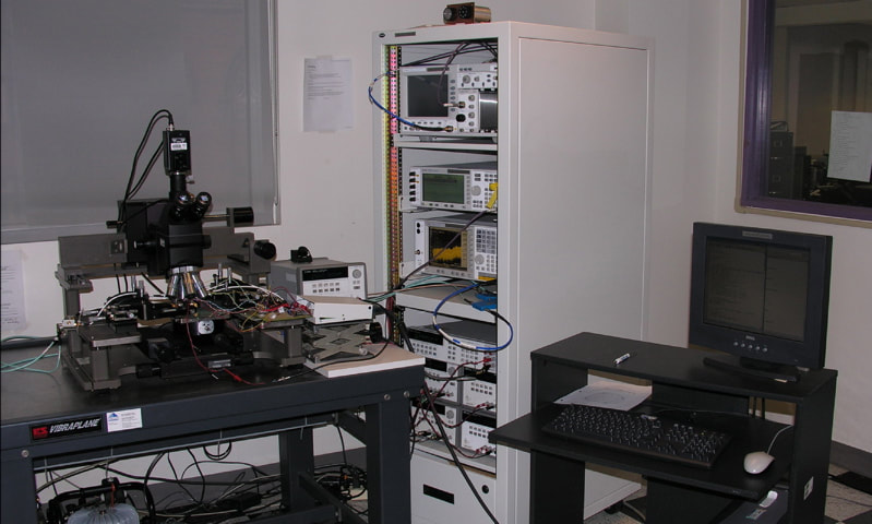
ANALOG & RF IC CHARACTERIZATION LABORATORY
|
Our lab facilities went through a substantial upgrade during 2004 and 2005 thanks to an NSF MRI Grant (with Prof. Tsividis) in conjunction with funding from Columbia University and the School of Engineering. We currently have a state-of-the-art measurement facility for IC characterization from DC to 40 GHz. We can measure on wafer circuits or packaged devices. Our instruments allow a full characterization in the frequency domain and time domain.
|
Copyright 2021 © Kinget Group. All Rights Reserved.